When we consider applying voltage onto a device, the first thing that comes to mind is connecting some electrodes and apply a time independent DC voltage. We can also consider an AC time-dependent waveform, such as a cosine function, through these contacts. But, of course, radiation is also made out of an electro-magnetic field and could bias our system as well. In fact, this way we can electrically bias the system with much higher frequencies (faster time scales) than we can achieve with electronic contacts. The field of terahertz (THz) optics strives to do precisely that – apply electric fields with few to tens of terahertz frequencies (1012 Hz) without physically contacting the sample under investigation.
Recently, the Leitenstorfer group had taken another important step in this path, generating a new type of THz waveform: a sharp step function [1]. We term this type of pualse a THz shockwave because of its resemblence to acoustic shockwaves. The electric field is constantly zero until at one time point it sharply rises to its peak value, within ~20 fs or 20*10-15 s (see blue line in the inset of the figure below).
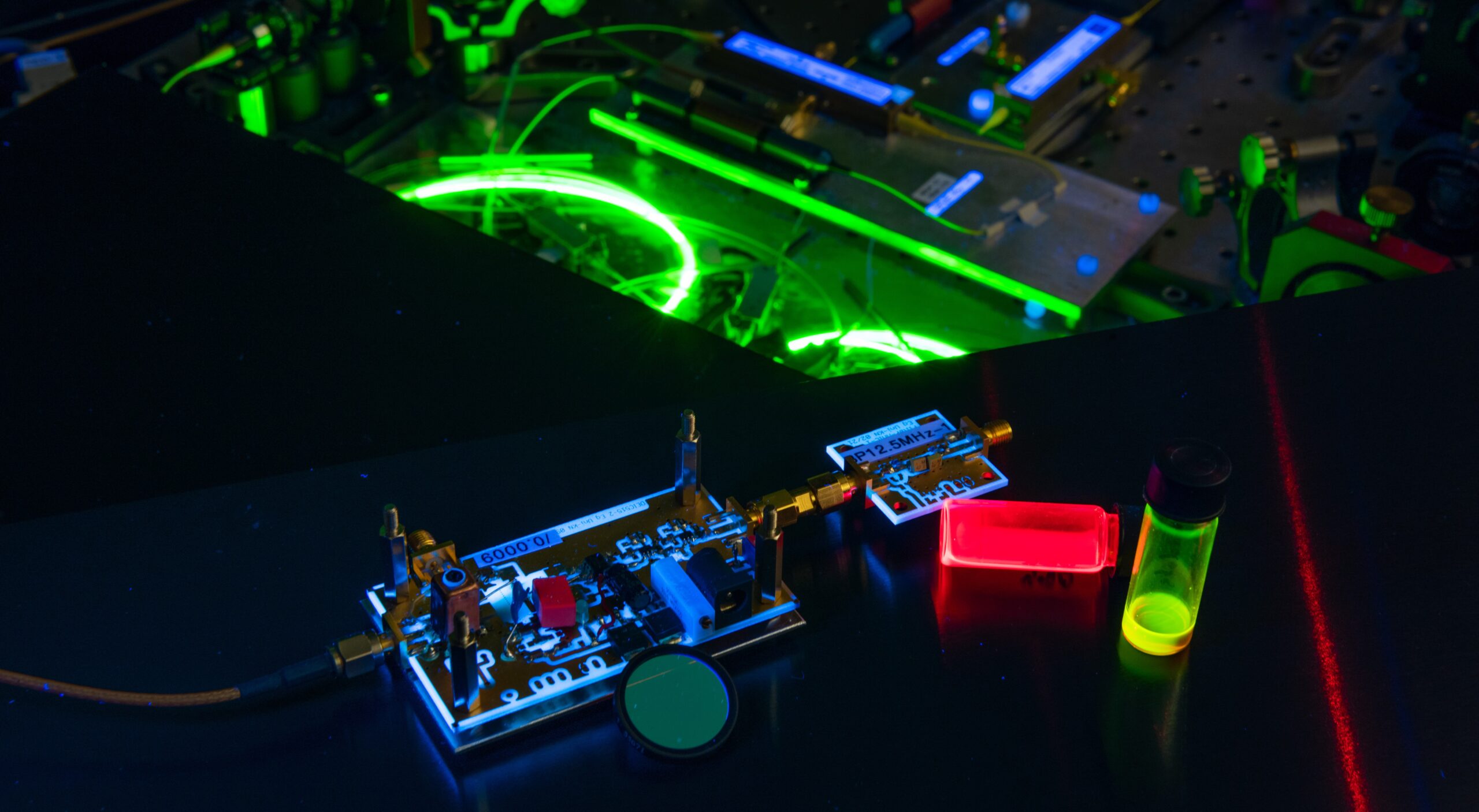
This pulse is synthesized by “slicing” of the original THz waveform. How does it work? In the figure below, a single cycle THz pulse (red beam) is created through optical rectification (OR) of the 775 nm wavelength pulsed laser. Then, this beam impinges onto a germanium (Ge) wafer positioned at the Brewster’s angle where no reflection occurs for the selected beam polarization (p polarized THz). However, when the arrival of the THz pulse onto the Ge surface overlaps with a short pulse in the visible range, something changes drastically! The visible pulse (green beam) excites electrons into the conduction band where they are quasi-free particles (electron-hole plasma). They are then accelerated by the oscillating THz field and radiate strongly in return. Now, most of the THz field is reflected by these free carriers (blue beam). The transition between the highly transmissive and highly reflective states happens within a few femtoseconds! This is how we get our shockwave. The inset shows a comparison of the waveforms of the original THz pulase (red dahsed line) with that of the shockwave (blue).

It is instructive to view the ‘slicing’ operation also in the frequency domain. A short step in time resutls in a very broad feature in the frequency domain (see bottom inset). This is a very unique feature as the shockwave continuously covers a frequency range from 0.2 THz to 30 THz – 7 octaves! Recently, we have used this source to follow the absolute density of free electrons in a narrow-gap semiconductor (InSb) [2]. Thanks to the large span of frequencies at our disposal, we could measure the electron plasma response (an oscillation of the electron/hole density). The plasma frequency (ωp) is important because it depends on the density of free electrons so if we measure it we have direct access to the time-dependent absolute density of electrons. On the other hand, the variation of this frequency is precisely why you need such a broadband laser source in order to measure it. With this method, we were able to show that both linear and nonlinear recombination routes are of importance for electrons in InSb.

Reflection spectra of the THz shockwave from a film of InSb, 300 ps after excitation with a 775 nm wavelength pulse. The spectra are taken under various excitation fluence (see label next to each spectrum). For higher fluonces, the density of free electrons increases and therefore also the plasma frequency (from 1 THz to 4.5 THz). The highly reflective feature at 5.5 THz results from the phonons of InSb.
[1] – Bühler et al. Optica 5, 7, 2018
[2] – Fischer et al. PRB 106, 20, 2022